NE565 NE 565 Phase Locked Loop IC PDIP−14
NE565 NE 565 Phase Locked Loop IC PDIP−14
Couldn't load pickup availability

- The range of power supply is wide
- Demodulated o/p is 0.2% linearity
- Power dissipation Max is1400mW
- Availability of linear triangle signal through in-phase zero crossings
- Operating voltage Max is ±12V
- Temperature ranges from -55ºC to +125ºC
- TTL & DTL compatible with the input of phase detector & output of square wave
- Hold in the range can be adjustable from ±1% to above ±60%
- The range of Operating Voltage ranges from ±5V to ±12V
- The stability of frequency for the VCO is 200 ppm/°C
- Range of Storage Temperature from -65°C to +150°C
- The current power supply is 12.5mA
- Max operating frequency of VCO is 500 KHz
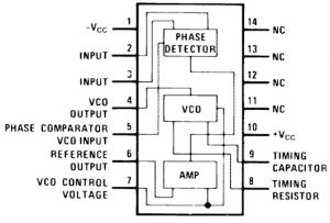
Pin Configuration
The pin configuration n of the NE565 Phase Locked Loop IC is shown below. This IC includes 14-pins where each pin and its functionality are discussed below.
- Pin1 (-Vcc): Input pin of the negative power supply
- Pin2 (Input): Input pin1 of the Phase detector
- Pin3 (Input): Input pin2 of the Phase detector
- Pin4 (VCO output): Output pin of the voltage-controlled oscillator
- Pin5 (VCO i/p of Phase comparator): Input pin of the phase detector
- Pin6 (Reference o/p): Reference o/p of Internal amplifier
- Pin7 (VCO control voltage): At this pin, the control voltage of VCO can be observed
- Pin8 (Timing Resistor): Resistor for running the frequency of VCO
- Pin9 (Timing Capacitor): Capacitor for running the frequency of VCO
- Pin10 (+Vcc): +Ve power supply
- Pin11, 12, 13 & 14 : No connection pins
Block Diagram
A Phase-Locked Loop IC mainly includes three blocks which include the following.
- Phase Detector
- Active Low Pass Filter
- VCO
In the above block diagram, a phase detector generates a DC voltage and this voltage is comparative to the phase dissimilarity among the input signal with frequency ‘fin’ & feedback signal with ‘fout’ frequency. It is a multiplier and generates two frequency-based components on its o/p like the two frequencies sum & difference of two frequencies.
An active LPF is a second component in the above blog diagram that generates a DC voltage on its o/p once the high-frequency component is removed which is present in the phase detector’s output. By using this, the signal can be amplified.
A voltage-controlled oscillator generates a signal with a certain frequency, once no input is provided to it. So, this frequency can be moved to any side by providing a DC voltage to it. Thus, the difference in frequency can be directly proportional to the DC voltage there at the LPF’s output.
The above processes occur until the frequency of the voltage-controlled oscillator is equivalents to the frequency of the i/p signal. So depending on the application, we can utilize either the o/p of active LPS otherwise VCO’s output.
Working of NE565 Phase-Locked Loop IC
In the block diagram of NE565 PLL, both the pins like 2 & 3 where the input analog signal connection can be done however pin2 are used as input whereas pin 3 is connected to GND.
Here, the input signal is given to the phase detector through VCO feedback which evaluates whether both signals are in similar frequency or not. If both the signals are in frequency, then the phase detector provides 0V output & if the frequency is there then this detector provides +Ve o/p voltage.
The phase detector’s o/p voltage is provided to an amplifier for amplifying the voltage signal & this can be given to voltage controlled oscillator. This oscillator produces a waveform where the frequency of this waveform mainly depends on the magnitude of specified input voltage.
When no input is provided to this, then the VCO in free-running mode will generate a signal. The frequency of this signal can be determined through the resistor and capacitor which are connected at pins 8&9.
Once an input signal is provided, then both the input signal frequency & the o/p of VCO can be evaluated. If they are not equal, the phase detector will supply a voltage and that is changed and given to VCO.
So, the signal frequency can be increased or decreased based on the voltage fed to an amplifier. When the modification is done then both the frequencies of the i/p signal & VCO will be equivalent.
In this way, PLL IC functions, the o/p frequency signal of voltage controlled oscillator is always attempts to continue through the i/p signal frequency.
Shipping & Returns
Shipping & Returns
- Shipping Time:- Our orders are shipped within 24 Hours.
- Delivery Time:- 2-5 Days (Anywhere in India), 7-10 Days for remote location
- Shipping Partner:- Bluedart, Delhivery, Xpressbees, & India Post.
- Replacement:- Damaged During Transit, Missing Parts Or Item Mismatch.
- Return:- Item mismatch or parts missing etc.
- No return/Replacement will apply if the Product has been subject to misuse, static discharge, neglect, accident, modification, or has been soldered or altered in any way.
- We accept no responsibility for improper installation of our products. Electrical polarity must be properly observed in hooking up electrical components.