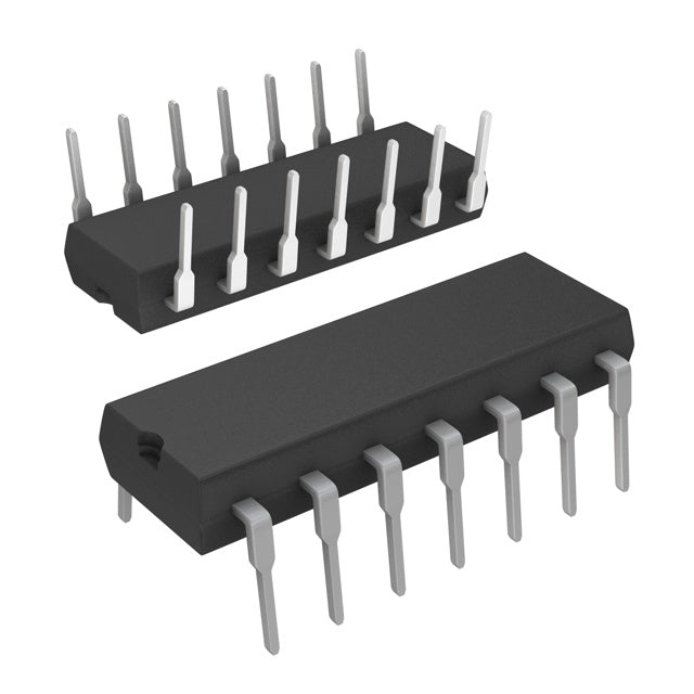
4011 CD4011 Logic IC, NAND Gate, Quad, 2 Inputs, 14 Pins, DIP
4011 CD4011 Logic IC, NAND Gate, Quad, 2 Inputs, 14 Pins, DIP
Regular price
Rs. 25.00
Regular price
Sale price
Rs. 25.00
Taxes included.
Flat Shipping calculated at checkout.
Quantity
Couldn't load pickup availability

CD4011 NAND gates provide the system designer with direct implementation of the NAND function and supplement the existing family of CMOS gates. All inputs and outputs are buffered.
Applications:
- Clock & Timing
- Consumer Electronics
Features:
- Propagation delay time = 60ns Typ. at CL = 50pF, VDD = 10 V
- Buffered inputs and outputs
- Standardized symmetrical output characteristics
- Maximum input current of 1A at 18V over full package temperature range; 100nA at 18V and 25C
- 100% tested for quiescent current at 20V
Shipping & Returns
Shipping & Returns
- Shipping Time:- Our orders are shipped within 24 Hours.
- Delivery Time:- 2-5 Days (Anywhere in India), 7-10 Days for remote location
- Shipping Partner:- Bluedart, Delhivery, Xpressbees, & India Post.
- Replacement:- Damaged During Transit, Missing Parts Or Item Mismatch.
- Return:- Item mismatch or parts missing etc.
- No return/Replacement will apply if the Product has been subject to misuse, static discharge, neglect, accident, modification, or has been soldered or altered in any way.
- We accept no responsibility for improper installation of our products. Electrical polarity must be properly observed in hooking up electrical components.